Hybrid CMOS/Nano Circuits for Ultra-Low Power Neural Networks
In recent years, the INTEGNANO research team has focused on leveraging resistive memory nanodevices as artificial synapses, closely integrated with computation to develop ultra-low power neural networks. This shift from fundamental research to practical demonstrators became feasible in 2017, as resistive memory technology matured to industrial levels, led by CEA LETI and microelectronics corporations. To facilitate this transition, a new integrated circuit (ASIC) design activity for hybrid CMOS/nanocircuits was initiated in collaboration with Jean-Michel Portal at IM2NP (Marseille) and Elisa Vianello at CEA LETI, building on prior CMOS design experience of the group.
This initiative was a cornerstone of the ERC project led by Damien Querlioz, with significant involvement from Jacques-Olivier Klein, aiming to reduce the energy consumption of deep neural networks (DNNs). DNNs, despite their remarkable success in fields like image recognition and automatic translation, are energy-intensive on traditional CPUs or GPUs due to extensive data transfers between processors and memory.
The team developed a hybrid circuit combining CMOS and memristor-based artificial synapses, achieving « in-memory computing » where memory and logic are intricately intertwined. This approach addresses the variability of memristors without the need for large error correction code (ECC) circuits, which would negate the benefits of in-memory computing. The ASIC chip, featuring a memristor matrix with differential bit structures made of HfO2, showed inherent error reduction similar to ECC without the overhead, significantly improving read speed.
Furthermore, the design facilitates the implementation of Binary Neural Networks (BNNs), enabling state-of-the-art AI performance with minimal memory requirements. The entire system, designed with Cadence IC tools and validated through simulation with measured data, exemplifies extreme energy efficiency, requiring nanojoules for tasks like handwritten digit recognition, compared to the micro-to-millijoules needed for CPU or GPU-based AI.
Unexpectedly, the robustness of this approach also allows for low-voltage programming of memristors, greatly enhancing endurance and enabling on-chip learning. Additionally, a novel effect was discovered, enabling a third weight state in memory points through read delay, offering a pathway to ternary networks and improved accuracy. This work underscores the importance of a holistic approach in modern micro/nano-electronics, from component physics to system-level applications.
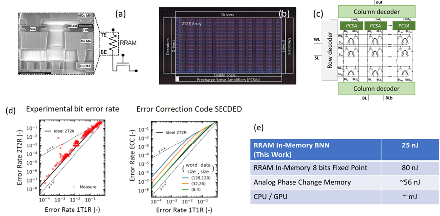
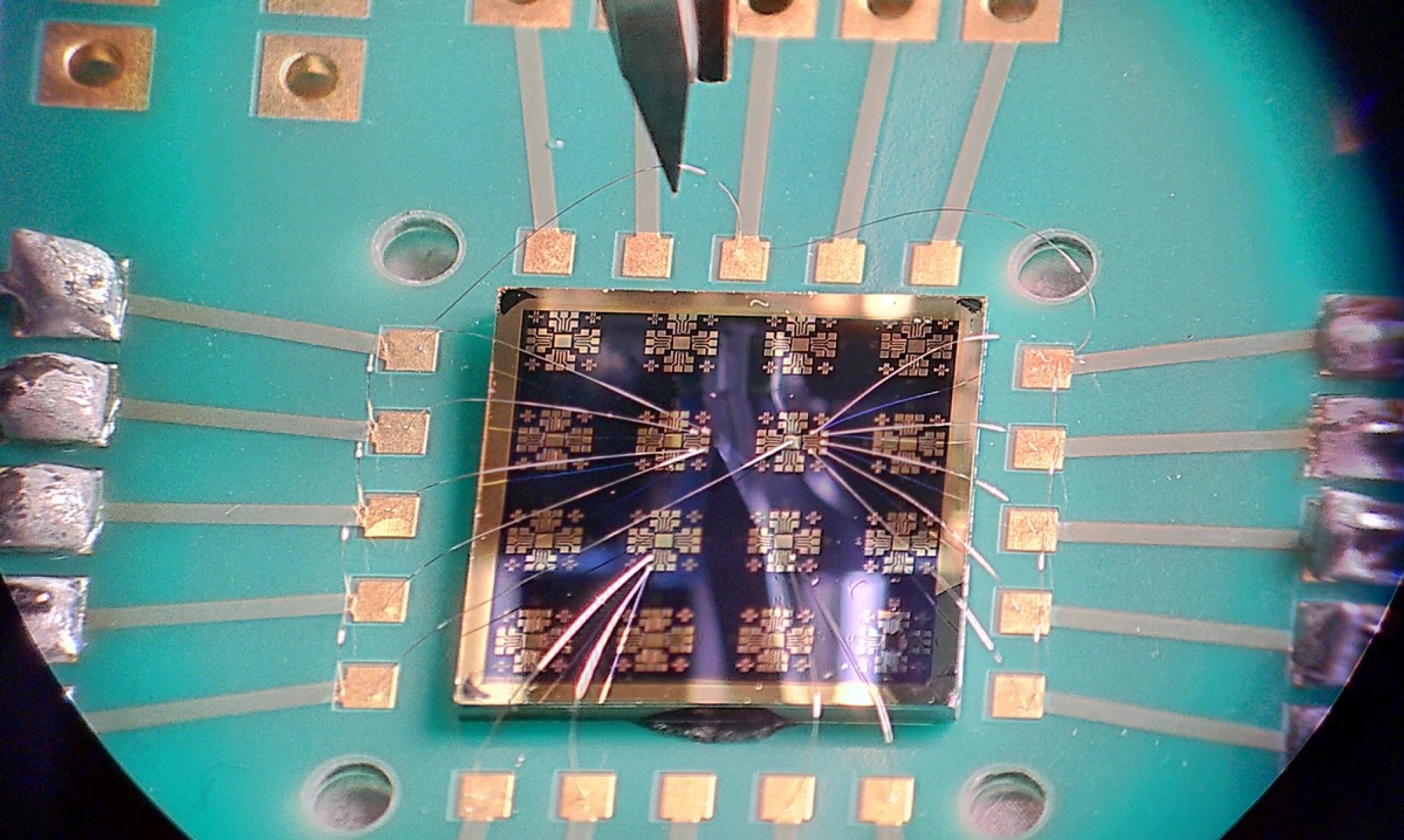
Fig 1: Results on BNNs. (a) SEM image of the utilized RRAM memristor technology. (b) Microscopic image and (c) diagram of our first demonstrator. (d) Efficiency of our differential technique in error reduction compared to a standard case (1T1R), alongside a comparison with traditional error correction codes (SECDED). (e) Energy requirement of our approach for recognizing a handwritten digit, compared to standard approaches.
Nanobayesian Electronics: Pioneering Ultra-Low Power Computational Models
Nanobayesian electronics is a particularly innovative design style, where nanodevices are treated as random variables: Imperfections of nanodevices, therefore, become features. Nanobayesian electronics aims at implementing Bayesian models, a type of highly explainable AI where the knowledge about variables is modeled using random variables.
The maturation of nanomemory technologies has significantly advanced the field of nanobayesian computation, culminating in the development of the largest nanobayesian system ever realized, in collaboration with LETI in 2019 and 2020. This system employs a memory matrix of 16,384 memristors integrated with CMOS peripheral circuits. The inherent stochasticity of memristors, due to atomic-scale conductive filaments, naturally implements the Monte Carlo Markov Chain (MCMC) Metropolis-Hastings sampling, a powerful Bayesian computing technique. This discovery led to the development of a method for executing MCMC using memristor physics, which was experimentally demonstrated to learn tasks such as cancer detection in mammography images with remarkable precision, comparable to software implementations of MCMC and neural networks, but with significantly lower energy consumption and fewer parameters. These findings were published in Nature Electronics.
In addition to the computational achievements, the team has explored another facet of nanobayesian electronics focused on inference, leading to the design of a more straightforward system potentially ideal for sensor fusion applications. Utilizing the hybrid CMOS/memristor technology similar to that used in binary neural network projects, doctoral students Tifenn Hirtzlin and Kamel-Eddine Harabi designed an ASIC chip, fabricated by LETI. This chip, the most complex integrated circuit designed in their laboratory to date, incorporates 30,080 transistors and 2,048 memristors, representing one of the closest integrations of memristors and CMOS globally. The design minimizes data transport over long distances, significantly reducing energy consumption related to interconnections. The fully functional system’s description and performance measurements have been accepted for publication by Nature Electronics.
These breakthroughs not only demonstrate the feasibility of nanobayesian systems for complex computational tasks with ultra-low power consumption but also highlight the potential for scalable and efficient AI models capable of on-chip learning and inference, marking a significant step forward in the integration of nanotechnology with traditional computing paradigms.
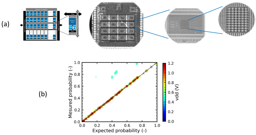
Fig. 2: (a) Diagrams and photographs of a hybrid CMOS/memristor ASIC implementing a reconfigurable nanobayesian circuit designed by my doctoral students and manufactured by LETI. This system closely integrates logic and memory. (b) Experimental measurements validating the functionality of this circuit.
Harnessing Physics for Computation: The Future of Neuroinspired Electronics
Collaborative efforts between the research team and Julie Grollier (UMR CNRS/Thales) have sparked innovative discussions on the future of neuroinspired electronics, particularly focusing on the potential of equilibrium propagation. This novel neural network training theory, developed by Yoshua Bengio’s group in Montréal (Turing Award recipient, 2018), presents a spatially local approach where the neural network is treated as a dynamic system. The network’s natural perturbations mimic a canonical artificial intelligence (AI) learning rule (gradient descent), making equilibrium propagation a biologically plausible alternative to traditional AI techniques.
INTEGNANO doctoral student, Maxence Ernoult, in collaboration with Bengio’s group, has made significant strides in adapting equilibrium propagation for hardware-centric logic. Their groundbreaking work was presented at the prestigious NeurIPS conference, ranking in the top 37 of 7000 submissions. This collaboration with one of the leading figures in AI has been notably impactful.
Further advancements were achieved by another doctoral student, Axel Laborieux, who addressed a numerical issue within this theory, thereby extending its applicability to more complex tasks. His work, co-authored with Yoshua Bengio, is considered a major contribution toward validating the equilibrium propagation approach, as published in Frontiers in Neuroscience.
Doctoral student Marie Drouhin has also done pioneering work on experimental physical systems based on memristors in the statistical measurement laboratory. These systems naturally learn through equilibrium propagation, marking a significant step towards realizing physically plausible neuroinspired computing models. This approach not only underlines the potential for creating energy-efficient, scalable AI systems but also highlights the integration of physical phenomena with computational processes, promising advancements in both the theoretical and practical aspects of neuroinspired electronics.